
SiC MOSFETs: A Game Changer in Power Electronics
Silicon Carbide Metal-Oxide-Semiconductor Field-Effect Transistors (SiC MOSFETs) are a game-changing invention in power electronics, outperforming traditional silicon-based transistors. These cutting-edge gadgets are made of silicon carbide (SiC), a material known for its outstanding characteristics, which open up new possibilities in power management.
Introducing A New Era of Efficiency
SiC MOSFETs stand out because of their distinct material features. Compared to silicon, silicon carbide has a larger band gap, allowing it to function at greater voltages and temperatures with exceptional efficiency. These results in lower switching losses and increased overall system efficiency, making them perfect for applications that require great performance and energy savings.
Compact And Powerful
SiC MOSFETs’ ability to tolerate higher voltages and currents enables smaller and lighter systems. This small decrease, along with their higher efficiency, makes them ideal for applications in which space and energy usage are crucial.
Optimizing Sic MOSFET Performance
Two researchers from the State University of New York Polytechnic Institute (SUNY Poly) in the United States claim to have achieved record-breaking performance for 4H-polytype silicon carbide (SiC) lateral metal-oxide-semiconductor field-effect transistors (MOSFETs).
Specifically, a 0.3μm-channel device with 2.5μm gate-drain spacing reached 7.7mΩ-cm2 specific on-resistance and 450V breakdown voltage. SiC-based devices aim to replace the more mature silicon technology for power integrated circuit applications, owing to a larger 3MV/cm critical electric field for breakdown, which is an order of magnitude greater than for silicon. The difficulty for SiC-based devices has been to obtain low on-resistances while maintaining high breakdown voltages. Devices were manufactured under a variety of process settings at the X-FAB 6-inch wafer foundry in the United States. The substrate had a 6μm highly doped n+ drift layer.
Aluminium ion implantation was employed to treat the distinct p-type areas.
The p-top region exhibited a single reduced surface field (RESURF) structure. In conjunction with the p+ body area, the p-top region formed a concentric floating field ring and junction-termination-extension structures for hybrid-JTE edge termination. The p-well enables accumulation and inversion-mode channels to be constructed. The accumulation mode produced reduced specific on-resistance (RON, sp).
The n+ source and channel-stop regions were created using high-temperature nitrogen ion implantation. The doping was activated with a 10-minute anneal at 1650°C under a carbon cover. Dry oxidation at 1175°C followed by annealing in nitric oxide (NO) resulted in gate insulation. After the gate oxide was patterned, the interlayer dielectric (ILD) was applied. Nickel was then used to develop a self-aligned silicide transistor manufacturing process. This was followed by rapid thermal annealing (RTA) at 900-1000 °C. Higher temperatures decreases contact resistance.
The device was completed with 4μm aluminum deposition for the source contact and gate pad, and nitride/polyimide front-side passivation. The device’s lateral architecture was made up of numerous interdigitated fingers that were centered on the source or drain. Edge-termination was not required for the source-centered designs, but it was required for drain-centered transistors to “alleviate crowding of electric fields at P+ regions in the periphery and extend the horizontal depletion layer to achieve the specified breakdown voltage of the device”.
Advantages
Silicon Carbide Metal-Oxide-Semiconductor Field-Effect Transistors (SiC MOSFETs) have emerged as game changers in power electronics, with a compelling set of benefits:
Superior Efficiency: SiC is more efficient than silicon due to its wider band gap, allowing for higher voltage and temperature operations. This leads to decreased switching losses and higher overall system efficiency, especially in applications with frequent switching cycles.
Compact Design: Compared to standard silicon MOSFETs, these devices can manage higher voltages and currents, resulting in smaller and lighter power electronic systems. This is especially useful for applications when space is limited.
Enhanced Reliability: SiC’s greater thermal conductivity enables effective heat dissipation, leading to increased reliability and a longer lifespan compared to silicon counterparts.
Environmentally friendly: SiC MOSFETs promote energy efficiency and reduce carbon footprint.
SiC MOSFETs provide substantial benefits in terms of efficiency, size, reliability, and environmental effect. However, their increased cost, gate drive complexity, and restricted availability must be carefully considered when making design decisions.
Applications
The extraordinary properties of SiC MOSFETs are revolutionizing several industries:
Electric Vehicles (EV): Their ability to manage high voltages and currents efficiently makes them ideal for EV power trains, resulting in extended driving range and faster charging periods.
Renewable Energy Systems: SiC MOSFETs can efficiently convert power from renewable sources, such as solar and wind, leading to a cleaner and more sustainable future.
Industrial Motor Drives: Their high performance makes them ideal for regulating industrial motors, resulting in increased efficiency and dependability in many industrial applications.
Power Supplies: SiC MOSFETs enhance efficiency and power density for electrical devices.
SiC MOSFETs offer a significant advancement in power electronics technology, setting the way for a future characterized by better efficiency, smaller size and improved performance across a wide range of applications.
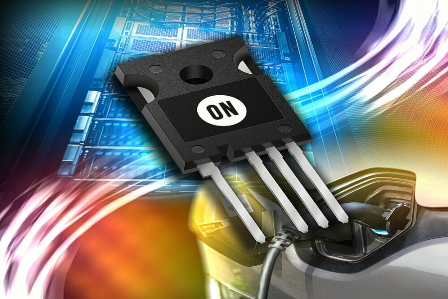
Featured image
Sources: